AI Chips: A100 GPU with Nvidia Ampere architecture

Nvidia GPUs have dominated the AI chip market for most of the decade. However, when Google’s TPU (Tensor Processor Unit) was publicly available in 2018 through the Google Cloud, it changed part of the competitive landscape considerably.

However, even in the scope of deep learning (DL), without a more detailed context, comparing TPU with GPU is like comparing an apple with an orange. In this series of articles, we will not perform any performance comparisons. Rather than passing judgment, my objective is to dive deeper into their corresponding architecture approaches. Besides GPU and TPU, we will look into the edge devices and other technologies like FPGA, that heavily invested by companies like Intel and Xilinx.
In part 1 of the series, we will focus on the GPU. The first half of this article involves the Nvidia GPU execution model and memory structure. Feel free to skip to the second half of the article if you know the background information, like CUDA, already — CUDA is the Nvidia platform for parallel computing and the programming model.
GPU execution model (optional)
As different GPU generations have slightly different designs and capabilities, let’s focus our discussion on the Ampere architecture introduced in 2020. But many discussions in this section are similar in the previous Turing (2018) and Volta architecture (2017).
Consider the following kernel “add” in a CUDA application (kernel — an application function to be run on the GPU device). This kernel adds one element from the array a and array b to array c (c[i] = a [i] + b[i]).

Say, each array a, b and c contain N=2²⁰ elements. In this implementation, “add” processes one element only. Therefore, to process a+b, we can spawn 2²⁰ threads in which each thread runs the same kernel code and be responsible for a single element. The element that it is responsible for will be identified by blockIdx and threadIdx above, which is implicitly set by CUDA.
In SIMD (single instruction multiple data), an instruction applies to many data elements concurrently. Nvidia GPU adapts SIMT instead (single instruction multiple threads). We can view a kernel as a sequence of instructions. Let’s say the next instruction is an INT32 op. Nvidia GPU groups 32 threads together and dispatch them to 16 INT32 arithmetic units to execute the instruction concurrently (or to 16 FP32 units for an FP32 operation).

Let’s explain this more precisely. Below is the code on the host CPU that launches the “add” kernel in the GPU.

To compute c, we need 2²⁰ threads. In CUDA, threads are grouped into blocks and the application can define how many threads each block has (up to a limit of 1024 threads). These blocks are required to execute independently in any order. This allows the GPU to scale with any number of cores. In our example, it defines each block contains 256 threads, and therefore, we need 4096 blocks ( 2²⁰/256). When a thread is processed, its block id and thread id (blockId and threadId) will be set implicitly by CUDA.
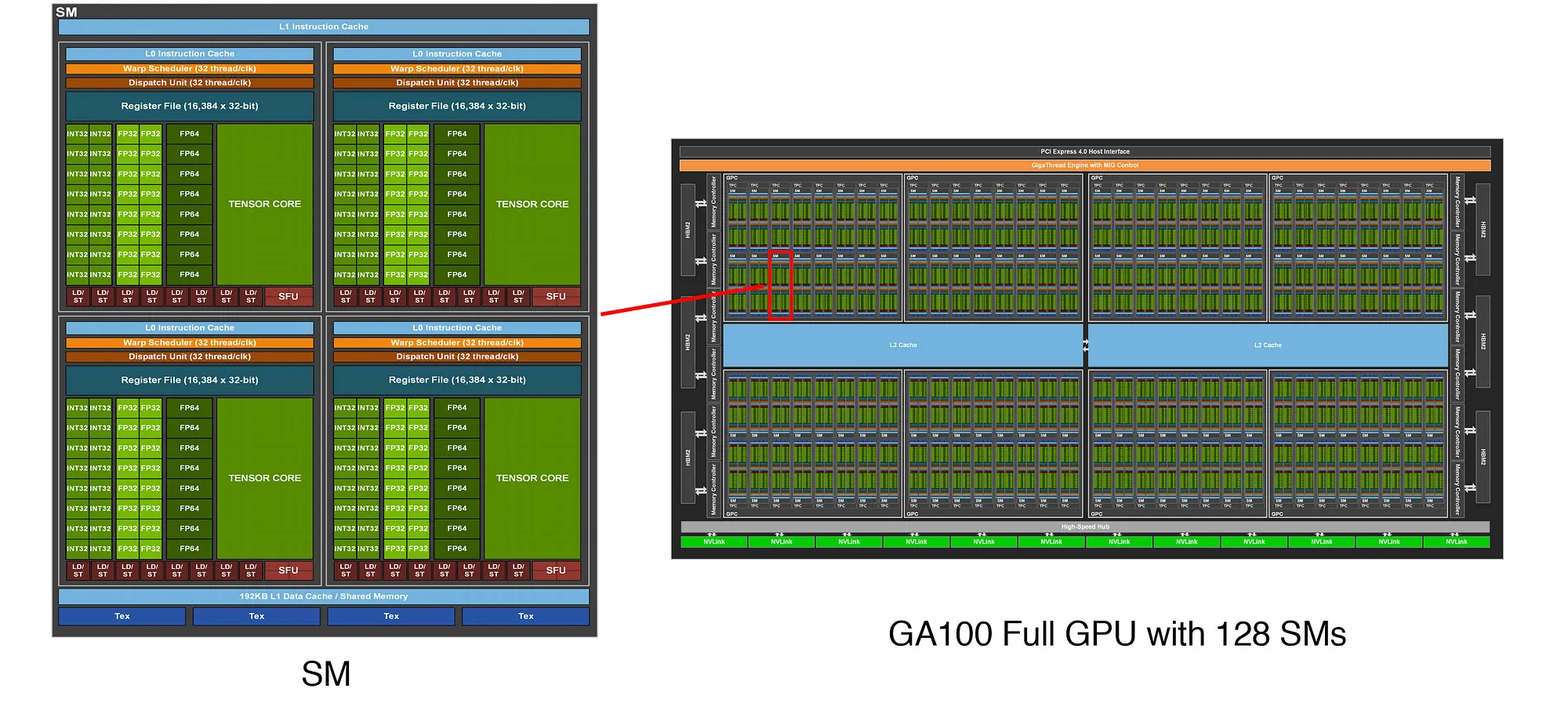
Each block will be assigned to a streaming multiprocessor (SM) in the GPU for processing. For the GA100 full GPU, it has 128 SMs.
Warp (optional)
A block stays in a single SM but SM does not manage its execution as a single unit. Instead, each block is further divided into warps that contain 32 threads each. In our example, each block has 256 threads, and therefore, each block has 8 warps (256/32). Ampere has 4 warp-schedulers. Each scheduler handles a static set of warps and at each clock cycle, it picks one ready to execute its next instruction. The warp will then dispatch to a dedicated set of arithmetic instruction units to execute one single instruction. For example, warp 1 of the block 4095, containing 32 threads, is scheduled by warp scheduler 0 to execute an INT32 operation on 16 INT32 units concurrently (or an FP32 operation on 16 FP32 units).

The diagram below from the Fermi architecture (2010) demonstrates how instructions are dispatched and executed in time (Fermi has only 2 schedulers).

The execution context (program counters, registers, etc…) for each warp is maintained on-chip during the entire lifetime of the warp. Register files, data cache, and shared memory are partitioned among the thread blocks. Therefore, in contrast to other context switchings, switching to another warp in the next time step has no cost penalty. But the predefined maximum number of blocks and warps that can reside in SM is limited by the GPU capacity. At every clock cycle, a warp scheduler issue an instruction that is ready to execute. This instruction can be selected from the same warp with no dependency on the last instruction, or more often an instruction of another warp. The execution time for many arithmetic instructions will take 2 clock cycles.
As shown below, multiple instructions can be executed concurrently. But the shown SM design is from Fermin which is different in Ampere. We just borrow the diagram for a high-level illustration. For example, the CUDA core in Fermi provides both FP and INT operations but Ampere separates them into INT32, FP32, and FP64 units. Execution time and the number of Schedulers are different also.

But by separating FP32 and INT32 cores (started in many GPU generations ago), it allows concurrent execution of FP32 and INT32 operations and increases instruction issue throughput. Many application loops contain pointer arithmetic in integer math with floating-point logic inside. Now we can process current FP32 operation while calculating pointer address for the next loop in parallel.
Branch divergence (optional)
CPU devotes a lot of die space to optimize control logic, like branch prediction and speculative execution optimization, to reduce instruction latency. GPU’s first priority is the threads’ instruction throughput, not the latency.
GPU has an ad hoc way in handling branching. As shown below, some threads may execute the “if” branch and some may execute the “else” branch depending on the value of the data a[index].

Both branches may be executed when processing a warp. When the “if” branch is processed, all threads that do not meet the “if” condition will be temporarily disabled (so as the “else” branch).

This branch divergence decreases the full utilization of the SM. If possible, to maximize throughput, all threads in a warp can be rewritten such that threads within a warp branch to the same code. Then only one branch will be taken and branch divergence will be avoided.
SM
Let’s get a more detailed view of the SM. In Ampere, SM contains four processing blocks that share an L1 cache for data caching. Each processing block has a Warp scheduler, 16 INT32 CUDA cores, 16 FP32 CUDA cores, 8 FP64 CUDA cores, 8 Load/Store cores, a Tensor core for matrix multiplication, and a 16K 32-bit register file. The maximum number of thread blocks per SM is 32.

Threads within a block can share data through shared memory with the same lifetime as the block. Shared memory is an on-chip memory with low latency. This is a big contrast to the global memory which is off-chip and has much higher latency and lower throughput.
SM provides very lightweight thread synchronization among threads in the same block also. To increase the execution efficiency, the kernel should take advantage of these capabilities within a thread block and reduce the need for global memory access and more complex synchronization.
Here is another view of issuing instruction and execution in the Volta architecture in a processing block (sub-core).

GPU Memory Hierarchy (Optional)
In a GPU device, data is physically stored in on-chip memory or device memory. Since device memory has lower memory throughput and higher latency, it is important to know where memory structures are stored as programmers have controls over it.
Global memory is large and accessible by all SMs. Treat it like the RAM of a CPU. But it is located in the device memory (off-chip) and is relatively slow. On-chip caches are provided to cache data for faster data access. Each SM has an L1 cache and at the GPU level, it has an L2 cache.

Each thread has access to dedicated on-chip registers. Registers are fast. Each thread has its own local memory acting as a spillover for registers or storing data structure that is too large or does not fit well with the register access model (like an array). However, local memory is stored in the device memory, and therefore, it is slow.

Focus on the use of shared memory in minimizing global memory access for a thread block. Shared memory is shared with threads of the same block. It is fast because it is on-chip. This behaves as a programmable L1 cache except the programmer has full control of what to store. If you plan the algorithm carefully, you can minimize the overall read from global memory. For example, break data shared within the same thread block to smaller chunks. If it can fit into the shared data, it reduces global memory read. (An example of how to do it for matrix multiplication can be found here.) The shared memory is also used to share data and results between threads in a block and for synchronization.

L1 cache, texture cache, and shared memory are backed by a combined 192 KB data cache in Ampere. Combining L1 cache with shared memory into a single memory block is done since Volta and it is shown to improve performance significantly. The portion of the cache dedicated to shared memory can be configured at runtime. At last, there is constant memory resided on device memory and cache to store constants.
Nvidia Ampere architecture with A100 GPU
The GA100 GPU has 128 SMs. A100 GPU only exposes 108 SMs for better manufacturing yield. The full implementation of the GA100 GPU includes
- 8 GPC and 16 SM/GPC and 128 SMs per full GPU.
- 6 HBM2 stacks and 12 512-bit Memory Controllers.

For each SM, Ampere has
- 4 processing block/SM, 1 Warp scheduler/processing block.
- 64 FP32 CUDA Cores/SM and 8192 FP32 CUDA Cores per full GPU.
- 64 INT32 CUDA Cores/SM, 32 FP64 CUDA Cores/SM.
- 192 KB of combined shared memory and L1 data cache
- 1 Tensor Cores/SM and 512 Tensor Cores per full GPU.
Here is peak performance for different operations.

Third-Generation NVIDIA Tensor Core
Google is not the only one in creating a complex instruction for matrix multiplication. Nvidia Tensor Cores (introduced since Volta) accelerate Mixed Precision model training that uses a combination of FP32 and FP16 math. Experiments show that many operations, like matrix multiplication, can be done in FP16 in many model training after taken some precautions. This reduces memory bandwidth and improves performance quite significantly.
Large matrics can be broke down into tiles with the result computed in a pipeline. Tensor Cores calculate a matrix multiplication followed by an addition.

It performs

in a pipeline animated in the next 20s in the video below.
Each SM includes four Tensor Cores. An A100 Tensor Core executes 256 FP16 FMA (fused multiply-add) operations per clock, allowing it to compute an 8×4×8 mixed-precision matrix multiplication per clock (multiplying 8×4 matrix with 4×8 matrix).
Ampere Tensor Core actually supports many data types including FP16, BF16, TF32, FP64, INT8, INT4, and Binary. The lower precision data type can be used in certain inferencing for faster performance. The high precision is for machine learning algorithms in which high precision is required.
TF32 is added to Ampere to emulate FP32 training with 16-bit math. TF32 covers the same data range of FP32, but with less precision. By default, TF32 tensor cores are used and no changes to user scripts are needed. For maximum training speed, use FP16 or BF16 in mixed-precision training mode.

In short, Ampere contains a wide spectrum of data format and precision. Some experiments may need to find the sweet spot of your models. Here is the performance for different data types in the Tensor Cores.

Matrix sparsity
As quoted directly from the Ampere whitepaper:
NVIDIA has developed a simple and universal recipe for sparsifying deep neural networks for inference using this 2:4 structured sparsity pattern. The network is first trained using dense weights, then fine-grained structured pruning is applied, and finally the remaining non-zero weights are fine-tuned with additional training steps. This method results in virtually no loss in inferencing accuracy based on evaluation across dozens of networks spanning vision, object detection, segmentation, natural language modeling, and translation.
In many model training, to avoid overfitting, we encourage sparsity in the model or perform weight decay to keep many weights to be small. So weight sparsity is a desirable behavior in deep learning. Here, we can first train a regular dense model but then prune the model in a sparsity pattern that is easy to compress. In specific, for every 4 elements in a row, we only keep two non-zero values with others not used. Then we further retrain (refine) these non-zero weights.

The A100 GPU introduces a new Sparse Tensor Core instructions that skip the weights with zero values. With the sparse pattern above, the number of weights will be reduced by half. Then it is multiplied with the activation. This weight reduction will double the operator's performance.

MIG (Multi-Instance GPU) Architecture
Using GPUs in the datacenter for inference is sometimes like using a 30 ft. big rig to deliver your lunch. Nvidia Triton Inference Server allows running multiple models and processing a batch of requests concurrently. In addition, Volta Multi-process service (MPS) can run kernels and memcopy operations from different processes concurrently. Nevertheless, memory resources like the L2 caches and memory bandwidth are still shared. One process may consume too many resources and impact the performance of others.
But why not virtualize the GPU such that multiple virtual GPUs (GPU instances) are run with dedicated resources. That is the goal for MIG. MIG partition each A100 into as many as seven GPU Instances. Each instance has dedicated SMs with isolated paths through the memory system. That includes the on-chip crossbar ports, L2 cache slices, memory controllers, frame buffer memory, and DRAM address busses.
The separated configuration ensures QoS and fault-tolerance for multi-tenants in a cloud-based solution.

This is another example of creating 3 GPU instances.

The state information of the GPU slices in a GPU Instance can be saved and restored in another GPU instance to an equal number of slices. Therefore, jobs can be migrated into other instances. This can pack more jobs in low utilized instances and free up resources for larger jobs. This increases GPU utilization and provides better job management.
Memory Architectures
HBM2
A100 GPU includes 40 GB of HBM2 DRAM memory with 1555 GB/s memory bandwidth on the circuit board. To achieve high memory density, HBM2 does not restrict itself in 2-D. Instead, it stacks up DRAM dies vertically (3D).

The memory dies are linked using microscopic wires with through-silicon vias (TSV) and microbumps. TSVs are vertical electrical connections passing through a silicon die and microbumps connect them between layers. An 8 Gb HBM2 die contains over 5K TSV holes. Then there is a silicon interposer underneath it responsible for routing signals between the DRAM and the GPU. Another layer of TSV and microbumps are used to connect these components to the package substrate that connects to the PCB board.

This packaging technology provides a wide memory bus lane with higher memory throughput and less power consumption comparing with GDDR6.
The memory in A100 is organized as five HBM2 stacks with eight memory dies per stack with error protection code to protect data. It delivers 1555 GB/s memory bandwidth.
L2 Cache
The A100 GPU also includes a 40 MB of L2 cache to increase performance (7x larger than V100 in Volta). The L2 cache is divided into two partitions to enable higher bandwidth and lower latency memory access. Each L2 is responsible for SMs in the GPCs directly connected to the partition. Hardware cache-coherence maintains the data consistency in the CUDA application across the full GPU.

Each L2 cache partition is divided into 40 L2 cache slices with size 512 KB each. A100 contains ten 512-bit Memory Controllers with which each controls eight L2 cache slices.
Asynchronous copy directly from global memory to shared memory
A new asynchronous copy instruction (used with a CUDA 11 asynchronous copy API) streamlines the data loading directly from global memory into SM shared memory. This bypasses the L1 cache and the use of register files to load the data into shared memory.

A100 L2 cache residency controls
We can view the DL inference as a one-directional computation graph with a stream of data. Intermediate results do not need to persist in the DRAM. For example, in inference, Ping-pong buffers can be persistently cached in the L2. In LSTM networks, weights are shared across GEMM operations that can be cached and reused.

In Ampere, we can set aside a part of L2 cache for persistent data. L2 persistence can be set up using CUDA Streams or CUDA Graphs. This memory space can be managed programmatically using an address range window also (see the CUDA document for details). With this cache management control, it ensures data are cached more efficiently and minimizing writebacks to memory and keeping reused data in L2.
Data compression
Ampere architecture also adds data compression to sparsity structure to speed up DRAM bandwidth. A100 Compute Data Compression improves DRAM bandwidth, L2 bandwidth, and capacity.

A100 improvement over V100
Here is a summary of improvement for A100 over V100 (Volta architecture) on the datapath, lower-precision math, and data sparsity handling.

NVLink
Nvidia continues beefing up its offerings in HPC (high power computing).

For your reference, this is the spec. for the DGX system.

One key design challenge is communications between devices and computers. Nvidia DGX uses the NVidia NVSwitch (an 18-port NVLink switch), Mellanox InfiniBand, and Mellanox Ethernet to scale clusters having hundreds or thousands A100 GPUs.
The fastest US supercomputer in 2020 is IBM Summit in the Oak Ridge National Laboratory. It uses NVLink 2.0 for the CPU-GPU and GPU-GPU interconnects and InfiniBand EDR for the system interconnects. According to Nvidia,
NVLink is a lossless, high bandwidth, low-latency shared memory interconnect, and includes resiliency features such as link-level error detection and packet replay mechanisms to guarantee successful transmission of data.
The third generation of NVLink used in Ampere has a data rate of 50 Gbit/s per signal pair and each link has 4 differential signal pairs (4 lanes) in each direction. A100 has twelve NVLink links with 600 GB/s total bandwidth.

DGX A100 systems can be connected with Mellanox InfiniBand and Mellanox Ethernet to scale up the data center.
PCIe Gen 4 support
As quoted from Nvidia:
The A100 GPU supports PCI Express Gen 4 (PCIe Gen 4) which provides 31.5 GB/sec of bandwidth per direction for x16 connections, double the bandwidth of PCIe 3.0/3. The faster speed is especially beneficial for A100 GPUs connecting to PCIe 4.0-capable CPUs, and for faster network interfaces, such as supporting 200 Gbit/sec InfiniBand for improved GPU cluster performance. A100 also supports Single Root Input/Output Virtualization (SR-IOV) that allows sharing and virtualizing of a single PCIe-connected GPU for multiple processes or Virtual Machines (VMs).
Other A100 features
A100 also offers:
- a 5-core hardware JPEG decode engine called NVJPG: It avoids decompression at the CPU level that may overload the PCIe.
- a GA100 Optical Flow Accelerator for optical flow and stereo disparity: Optical flow measures the apparent motion of points between two images, and stereo disparity measures the depth of objects from a system of two cameras.
CUDA 11 also provides new API for new features: including third-generation Tensor Cores, Sparsity, CUDA graphs (for quick launch and execution dependency optimizations), multi-instance GPUs, L2 cache residency controls, etc…
Credit & References
NVIDIA A100 Tensor Core GPU Architecture
Getting Started with Tensor Cores in HPC
Tensor Core DL Performance Guide
Dissecting the NVIDIA Volta GPU Architecture via Microbenchmarking
Volta: Programmability and Performance
NVIDIA’s Next Generation CUDA Compute Architecture: Fermi
NVIDIA’s Fermi: The First Complete GPU Computing Architecture