AI Chips Technology Trends & Landscape (Mobile SoC, Intel, Asian AI Chips, Low-Power Inference Chips)

At last but not least, we will cover the second half of the AI chip companies. This includes a wide spectrum of product offerings from Intel and the Mobile SoC (System on a Chip) from Apple, Qualcomm, and Samsung that comes with multiple Neural Processing Unit (NPU) cores. Then, we will go over chips that are specific for AI accelerations. In addition, Asian countries have put AI development as a strategic priority, so we will look into their offerings. Finally, we will close our discussion with one important and competitive market segment — the low-power AI edge devices.
Habana Labs
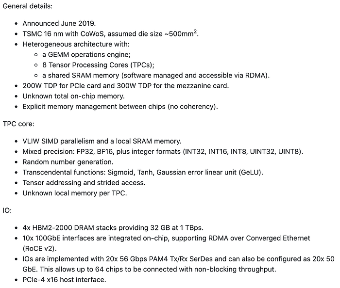
Intel acquired Habana Labs in late 2019 for 2 billion. Let’s see what Intel gets for the money. Habana Labs offers Gaudi for AI training and Goya for inference. A Gaudi 2000-HL chip contains a cluster of eight Tensor Processing Core (TPC) and an accelerated GEMM (matrix multiplication) engine (left diagram below). Each core supports VLIW SIMD in exploring instruction-level parallelism and data parallelism. It also supports mixed precision calculations.

In the HLS-1 system (Habana Labs System-1), it contains eight HL-205 OAM Mezzanine cards and each card contains a Gaudi 2000-HL chip with 4 HBM memories on a single-chip package.

Each chip implements ten ports of 100Gb Ethernet with the support of remote direct memory access (RDMA). In HLS-1, all chips are connected all-to-all on the PCB using seven 100Gb Ethernet ports. This design allows commodity networking equipment instead of a proprietary solution like Nvidia NVLink. This is the centerpiece of their strategy of using multiple Ethernet between nodes in training a large DNN that requires multiple nodes. The high bandwidth between nodes lessens the overhead of operations like reduce, all reduce, gather, and broadcast.
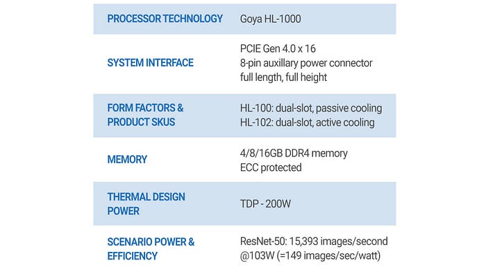
Habana’s Goya, with the HL-1000 processor, is dedicated to inference workloads.

Specification (Optional)
Here is the general information available from a third-party source on the Gaudi processor.
This is the specification for the Goya inference card:
Intel
Intel has a wide spectrum of product offerings in AI, including those billion dollars acquisitions.
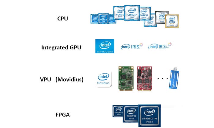
They are
- CPU with MKL-DNN: MKL-DNN is a math kernel library in accelerating DNNs.
- Integrated GPU: Utilize on-chip processor graphics.
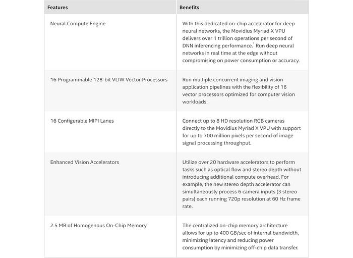
- VPU Movidius: Used in machine vision for low power devices.

Movidius includes hardware accelerators for both DNN and imaging/video pipeline.
- Agilex, Stratix FPGA
Microsoft’s Project Brainwave accelerates DNN inferencing in major services such as Bing’s intelligent search features and Azure.

Brainwave applies Intel Stratix 10 FPGAs for its NPU (neural processing unit) design for real-time AI. This NPU has a SIMD vector processor architecture. It contains a dense matrix-vector multiplication unit capable of processing low batch inferencing with high utilization. There are other units that perform element-wise vector-vector operations and activation functions. Stratix 10 FPGAs are picked for its implementation because of the short-latency focus on the FPGA.

- Habana Labs Gaudi and Goya (discussed in the last section).
Intel’s diverse product offering can be a major headache for developers and its AI strategy. To address this heterogeneous environment, Intel offers OpenVINO to code and deploy the inference in a device-agnostic way. Each type of accelerator will provide a runtime plugin to handle the difference automatically. In addition, multiple inference pipelines can be distributed and run on different devices in parallel.

Intel also proposes OneAPI as a device-agnostic programming model for parallel computing. It can be viewed as a competitor to NVidia CUDA, but for any hardware accelerator.
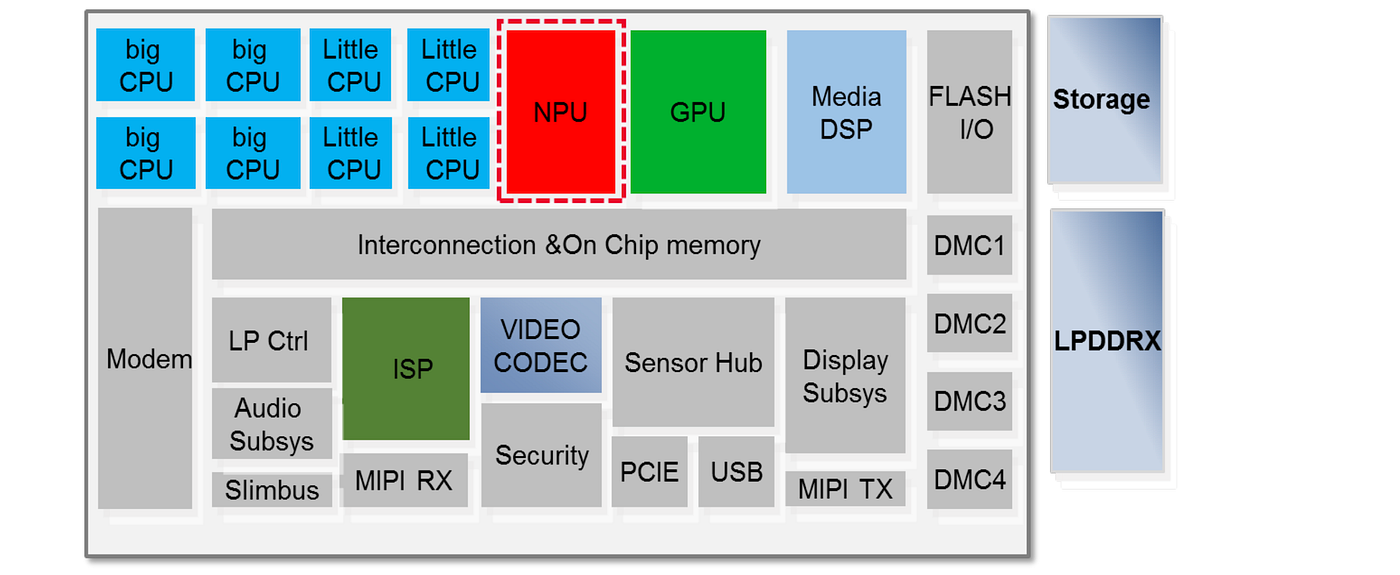
Mobile AI Chip
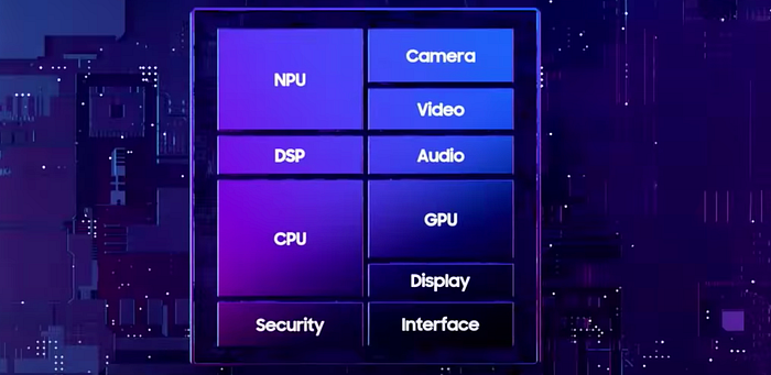
The most commercial success chips with AI cores are the ARM-based SoC (system on a chip) used in mobile phones. These chips have multiple cores of CPU and GPU with the key objective of delivering the highest performance per watt. The CPU cores are categorized into clusters. There will be at least one prime core with the highest computation power at a high clock rate and core(s) for energy-efficient computing. For some design, there will be cores with power in between these two. These CPU cores are often enhanced with complex instruction sets accelerating the vector and matrix (tensor) operations. These chips also include multiple Neural Processing Unit (NPU) cores in accelerating operations in machine learning and deep neural networks (DNN). They also have an image signal processor (ISP) in processing camera sensor data, and special components in image/video/audio processing, cryptography, and power management.
Unfortunately, many architecture designs are well-kept industrial secrets and therefore, we can only go through some of their high-level information.
Apple

Apple A14 Bionic (2020) is a 64-bit ARM-based SoC with
- 11.8B transistors using the TSMC 5nm process,
- A six-core ARM CPU with two high-performance cores and four energy-efficient cores. It has a wider superscalar design and a larger cache than the predecessors,

- With matrix multiplication accelerations in CPU cores,
- A 16-core Neural Engine (changed from 8-cores in A13) at 11 TOPs,
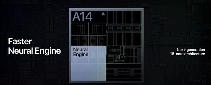
- A new architecture for the four-core GPU.
The major changes over the A13 Bionic chip are the use of 5 nm fabrication, doubling of Neural Engine performance, and larger caches.
Qualcomm
Qualcomm Snapdragon 865/865+ is an SoC announced in 2020. The Kryo 585 CPU unit contains a Cortex-A77 core at 2.84 GHz, three Cortex-A77 cores at 2.42 GHz, and 4 Cortex-A55 cores for power saving.
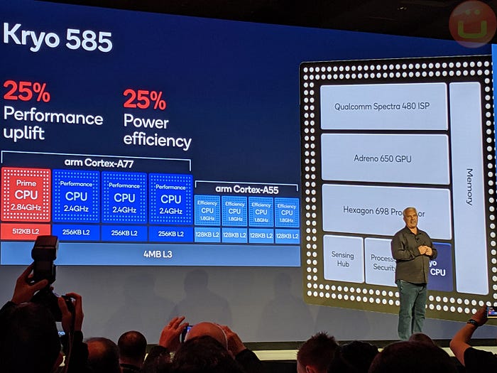
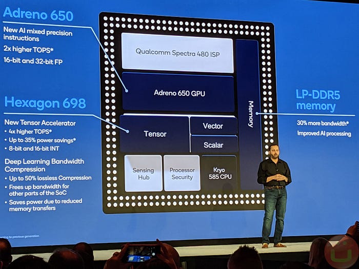
It also includes Adreno 650 as GPU and Hexagon 698 as DSP/NPU for scalar, vector, and tensor acceleration.
Here is the high-level specification.
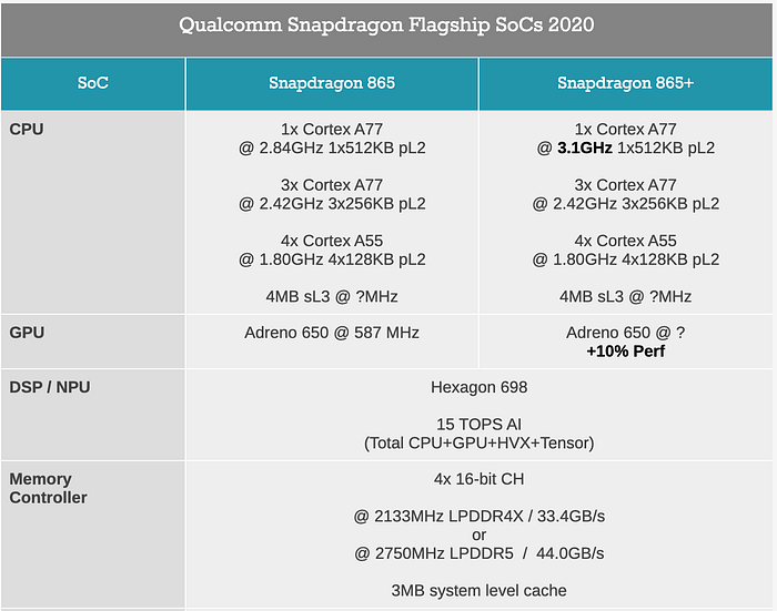
Snapdragon 865+ has a maximum clock speed of 3.1 GHz. It has 1.8 MB level 2 cache, and 7MB level 3 cache. It uses TSMC 7nm process (N7P) and has a die size of 84 mm².
Samsung
Samsung Exynos 990 processor (2020) contains a dual Samsung custom M5 core for peak performance, two additional ARM Cortex-A76 for high-performance tasks, and four small and power-efficient ARM-Cortex A55 cores. It also contains a dual-core NPU.
It has a 4MB cache and a maximum clock speed of 2.7 GHz. It has a die size of 91.8 mm² and it is manufactured by Samsung itself using 7nm LPP (with EUV) process.
Huawei/HiSilicon
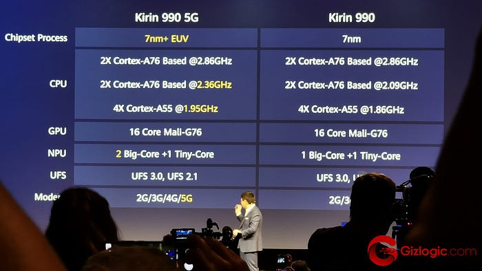
HiSilicon Kirin 990 5G (2019) contains two Cortex-A76 cores with up to 2.86 GHz, two Cortex-A76 cores up to 2.36 GHz, and four small ARM Cortex-A55 cores for power saving. It has a 16 core Mali-G76 GPU and 2 + 1 Ascend cores as NPU. Here is the high-level specification.
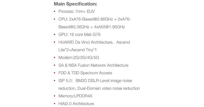
It has 10.3B transistors on a 113.3 mm² die. It is manufactured with TSMC 7nm process (N7P).
Arm
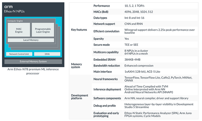
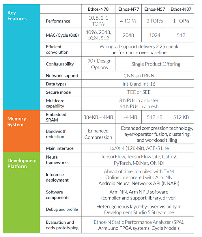
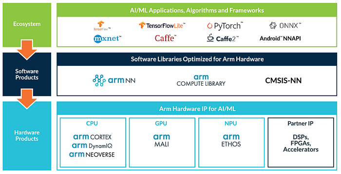
Many Mobile SoC ships and AI chips ship with ARM cores (Cortex) and ARM GPU cores (MALI). ARM also provides Ethos-N78 (NPU cores) for ML acceleration. Nvidia proposed to purchase Arm. This shows its importance in the field. Here is its specification from Arm (MAC stands for Multiply-Accumulate Operation).
Specification (Optional)
This is the specification for Arm different offerings.
Arm NN software
The open-source Arm NN software and Arm Compute Library bridge between common DL frameworks and the underlying Arm processing hardware, such as CPUs, GPUs, or Arm machine learning processors. Many Arm hardware IPs below are integrated into SoC in many products discussed in this series of articles.
AI Chips
Next, we will look at chips specifically for ML/DL accelerations.
Huawei/HiSilicon
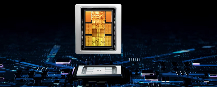
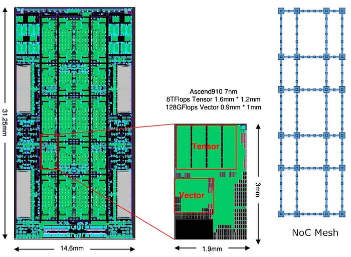
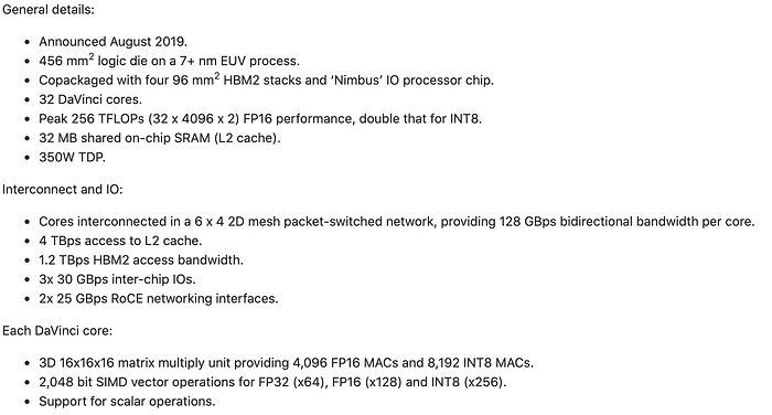
HiSilicon Ascend 910 is an integrated SoC processor including CPU cores, Da Vinci AI cores, DVPP (digital vision pre-processing). The processor delivers 256 TFLOPS for FP16 and 512 TOPS for INT8 with 350 W of max power consumption. This is the block diagram for Ascend 910 which puts 32 Da Vinci AI cores on the same die with 32MB on-chip HBM2 L2 cache.
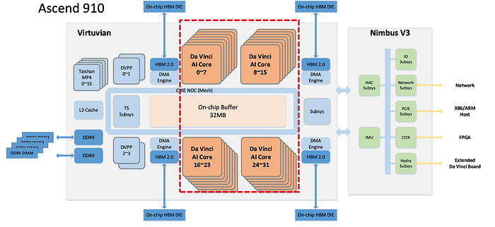
The Da Vinci AI cores contain a scalar unit and a 2048 bit INT8/FP16/FP32 vector unit with special function support (like activation functions, NMS Non-Maximum Suppression, ROI, SORT).
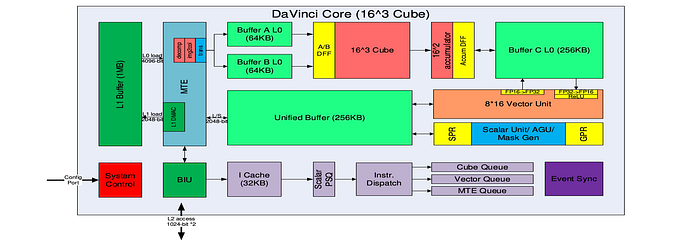
There is another 3D Cube Engine for matrix (16x16x16) operations. It can perform 4,096 FP16 MAC operations (¹⁶³) per clock cycle.
Packaging (Optional)
Packaging technology for Ascend 910 is important in minimizing latency and maximizing throughput between die. The AI SoC is composed of 8 dies integrated together (two dummy dies for the mechanical reason).
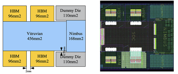
The AI SoC die stacks above the 3D-SRAM as the AI core cache. Then stacks of HBM2E memory are connected to the SoC through the underneath silicon interposer.

NoC (Optional)
The red rectangle below is a single core out of the 32 Da Vinci AI cores in Ascent. A Mesh NoC (Network-on-chip) connects these cores together providing 128GBps read and 128GBps write per core. This 1024bits 2GHz NoC Mesh (on the right below) access on-chip L2 cache at 4 TByte/s and off-chip HBM at 1.2 TByte/s.
Ascend 910 AI Server Cluster
An Ascend 910 AI Server contains 8 Ascend 910 and an Ascend 910 Cluster contains up to 2048 nodes (2048 Ascend 910).

SoC and Edge device
The Da Vinci cores also integrate into Mobile SoC like Kirin 990 5G as its NPU.
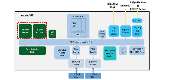
Ascend 310 is designed for edge inferencing with 2 Da Vinci AI cores. It can operate at 16 TOPS for INT8 and 8 TOPS for FP16. It consumes 8W of power only.
Specification (Optional)
Here is the general information available from a third-party source.
Cambricon
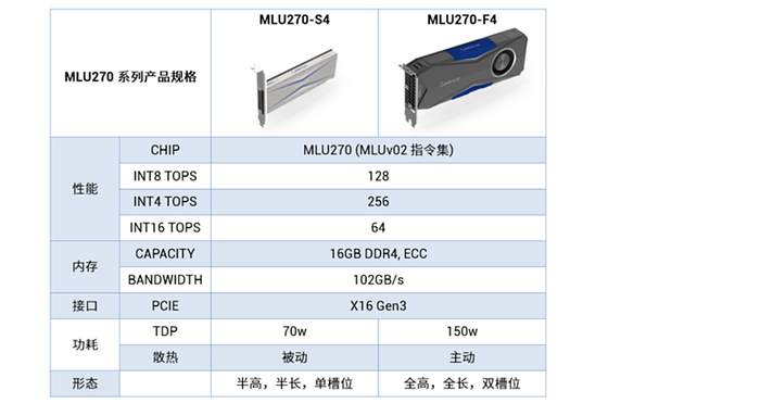
MLU 270 (思元270) is a neural processor for cloud-based workloads in inferencing and training. It provides INT8 (128 TOPS), INT4 (256TOPS) INT16 operations (64 TOPS), FP16 and FP32 including mixed-precision. Utilized specially designed algorithms, MLU 270 emphasizes on low precision fixed-point arithmetic for model training. It has 16 cores with hardware-based data compression to improve the capacity and bandwidth of the cache. It supports 48 streams of video decoding (1080p30) and 16 streams of video encoding. It is manufactured by TSMC with the 16 nm process. Here is the specification for two acceleration cards using MLU 270.
MLU 270 has four clusters with 4 cores each. All cores are connected to the network-on-chip (NOC) with passage to four DDR controllers and each containing one channel. The whole system has access to 16/32 GB DDR4. Each core contains a functional unit (FU), a general register group (GPR), a neuron storage unit (NRAM), and a weight storage unit (WRAM) (storage≡memory here).
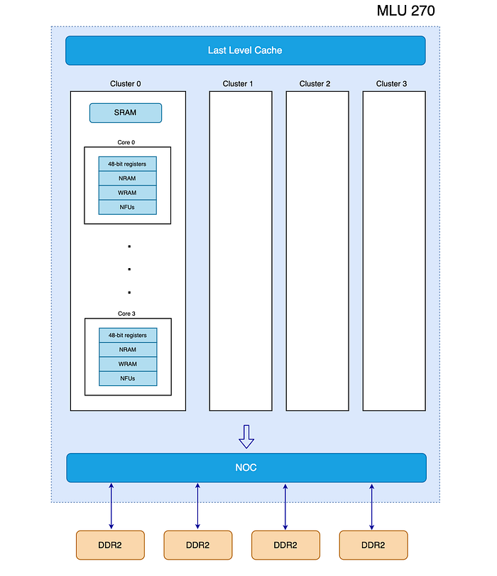
The system has different levels of memory. Developers can declare where data is stored. Each core has 48-bit registers for scalar data. It also has Neural-RAM for storing scalar or stream data (scalar or tensor). It is on-chip RAM with 512KB/core. Weight-RAM (tensor) is an on-chip RAM that stores model weights with 1MB/core. Every 4 cores shared a Share-RAM (SRAM) which has the size of 2MB. It has off-chip DDR and used for Global-DRAMS and Local-DRAMS. Every core has access to its own Local-DRAMS but cautious that this is off-chip memory. There is a Last Level Cache (L1 cache) with a maximum size of 2MB. It mainly uses for buffering shared read-only data, instead of off-chip memory access.
MLU 290 is also announced in 2020. It has 64 cores and 32GB HBM2 storage at 1024GB/s with 512 TOPS. It is fabricated with the TSMC 7nm process.
MLU220 is a neural processor for edge computing. The product integrates 4-core ARM CORTEX A55 with 2/4/8 GB LPDDR4x memory. It has 16 TOPS for INT8.
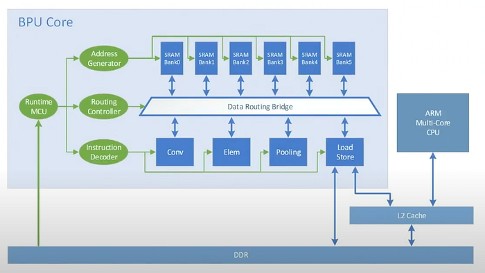
Horizon Robotics
Horizon Robotics Journey 2 (征程) is an AI processor in the automotive industry and Sunrise (旭日) is mainly for smart camera. Both chips are designed for edge devices in inferencing.
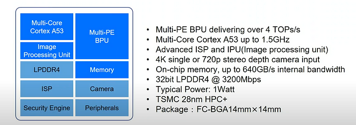
Here is the architecture for the BPU core (Brain Processing Unit). It is a 64-bit MIMD using 24 stages pipeline.
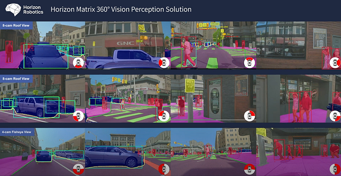
Here is some demo in applying the technology.

And the Matrix is its autonomous driving computing platform using Journey 2.
MediaTek
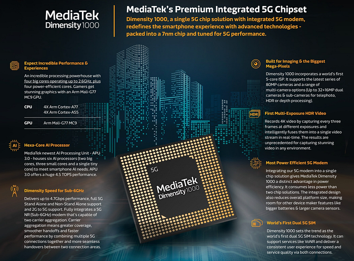
MediaTek 5G SoC Dimensity 1000 (天璣 1000) embeds a six cores AI processor (MediaTek APU 3.0 achieving 4.5 TOPS) — 2 big cores, three small cores, and a tiny core for facial recognition.
Below is some snapshot from the promotion video for Helio P90 APU (曦力P90) on AI applications, including AI beauty retouching.


Here is a short video of using pose tracking to animate an avatar or control a robot.
Alibaba
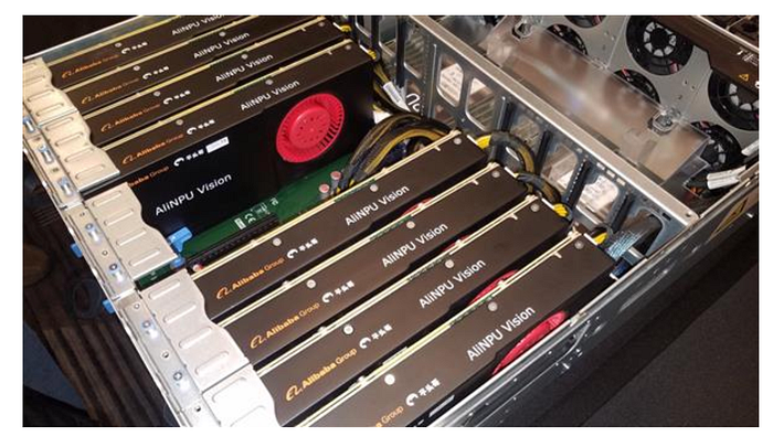
Alibaba Hanguang 800 (含光800) is an NPU designed for inference in their data centers and edge servers. It has 17B transistors fabricated by TSMC 12 nm process. It can process 8,563 IPS (Image Per Second) with power efficiency at 500 IPS/W. This chip has the first key deployment in AI computer vision. It accelerates convolution, 3D-convolution, matrix multiplication, transposed convolution, dilated convolution, and ROI with focuses on DNNs like ResNet-50, SSD/DSSD, Faster-RCNN, Mask-RCNN, and DeepLab. It has the direct support of activation functions including ReLU, sigmoid, tanh, etc …
Contrary to many AI chips design, GEMM engine design is not used. The designers argue in this paper that
Computing CONV on a GEMM engine, one needs the img2col() transformation to flatten images into general matrixes. This introduces huge data inflation, leading to unnecessary extra computation and storage, but also decreasing arithmetic intensity and bounding performance towards I/O and memory.
Like many designs, it supports low arithmetic precisions including INT8, INT16, FP16, and BF16 to reduce memory requirements. With direct hardware support, it also takes advantage of model sparsity (weights compression) and quantization. This memory strategy fits the model operations within the internal 192MB SRAM (such that it can minimize I/O without external memory). All these optimizations are proven to be significant in improving inference throughput compared with other alternatives. This also streamlines many existing operations and power consumption for Alibaba services.
Baidu
Baidu Kunlun (昆仑) is based on its XPU neural processor architecture that contains thousands of small cores for AI computing in the cloud and on the edge of networks. The chip performs up to 260 TOPS at 150 Watts with two HBM2 at 512 GB/s. Kunlun is fabricated by Samsung using 14 nm process technology.
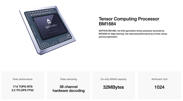
Bitmain/Sophon
Sophon is a family of low-power NPU. BM1684 is its high-performance product.
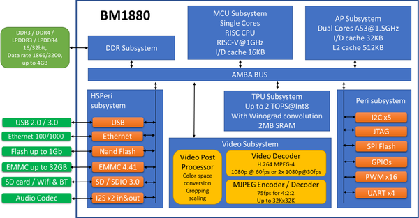
BM1880 TPU provides 1 TOPS computing power with int8, and up to 2 TOPS computing power with Winograd convolution acceleration. It has a single-core RISC-V MCU subsystem with a dual-core Cortex-A53 along with a TPU subsystem using 8-bit integer arithmetics.
Rockchip
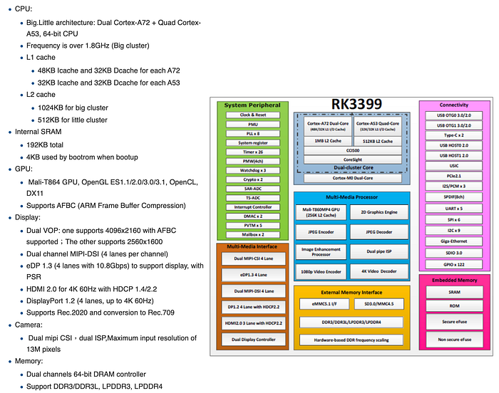
Rockchip RK3399 SoC integrates dual-core Cortex-A72 and quad-core Cortex-A53 with a separate NEON coprocessor and with ARM Mali-T864 GPU.

Specification (Optional)
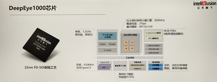
Intellifusion

DeepEye1000 operates at a peak of 2 TOPS with INT8/12/16 operations.
Eyeriss
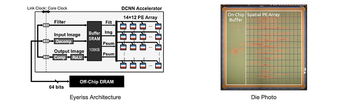
Eyeriss is an MIT project on studying the design of an energy-efficient CNN accelerator. The test chip contains a spatial array of 168 processing elements (PE) fed by a reconfigurable multicast on-chip network. It minimizes data movement by exploiting data reuse. The major reason for me to include this in our discussion is its heavy study on where and how to save power (detailed in a video presentation on energy-efficiency).
Performance/Watt
These energy-conscious designs lead to another type of startups that focus on performance per Watt instead of raw performance.
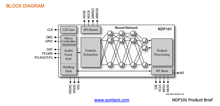
Syntiant

Syntiant NDP101 Neural Decision Processor is an ultra-low-power processor for always-on speech detection (event detection) and audio recognition. It replaces buttons, switches, and dials for devices to wake up by words rather than touch.
It has a general-purpose ARM Cortex-M0 processor with 112KB SRAM. It is good for applications that require an MCU for control and a neural engine for decision making.
Hailo
The Hailo-8 processor features up to 26 TOPS and 3 TOPS/Watt.
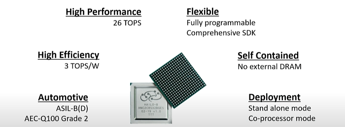
And it utilizes the data flow architecture that we discuss in part 1.
It is highly likely that the inference is done in low-precision calculations (this video from Hailo demonstrates some concept of doing 8-bit Deep Learning).
Kneron
Kneron KL520 is an NPU designed for edge devices. It is optimized for CNNs and runs 0.3 TOPS at 0.5 W which is adequate for facial recognition for security applications like smart door locks. It includes two ARM Cortex M4 CPU. It also contains a custom Kneron NPU.
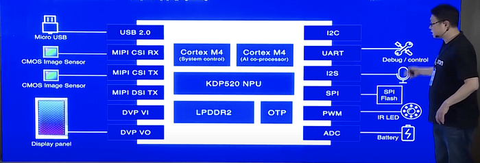
The higher-end Kneron KL720 AI SoC comes in at 0.9 TOPS per Watt for both computer vision and NLP. The average power consumption for the full package is around 1.2W.

Mythic
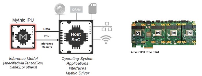
Mythic IPU adopts the dataflow architecture using an array of tiles. Each tile includes multiple units: a Matrix Multiply Accelerator (MMA), a RISC-V processor, a SIMD engine, SRAM, and a Network-on-Chip (NoC) router. The MMA is done with analog computing coupled with embedded flash memory. It tunes the value of resistors according to weights and uses the input value to control the voltage. The calculation outputs will be in the form of the output currents. The SIMD unit provides operations such as maximum and average pooling. The SRAM holds program code and data buffers and the RISC-V manages the tile scheduling.
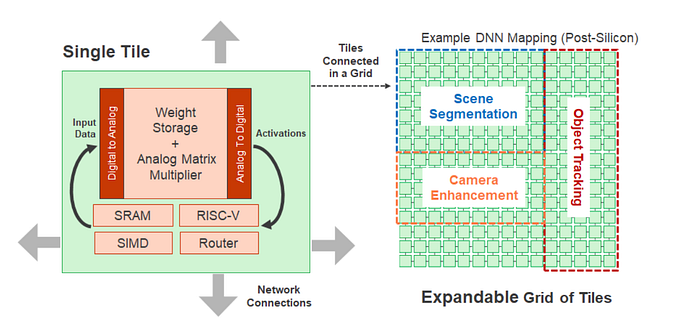
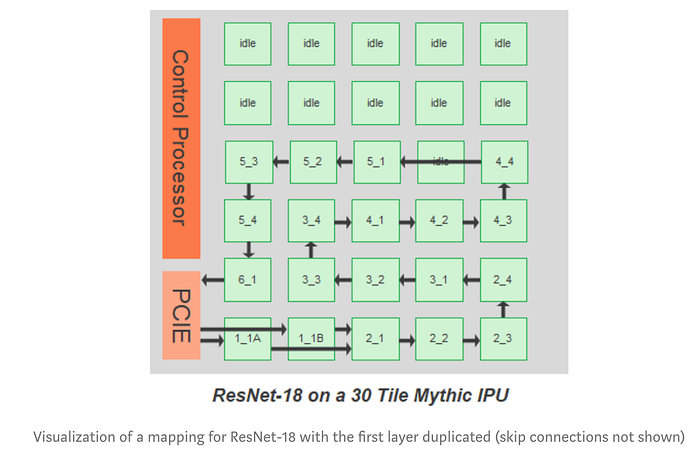
And this is a visualization of mapping ResNet-19 into the pipelines created by connecting tiles.
Here is the general specification:

Perceive
Perceive’s Ergo can process large DNNs in 20 mW with 55 TOPS/Watt. It requires no external RAM in a small 7x7 mm package. According to Perceive, it delivers over 4 TOPS peak performance at less than a tenth of a watt peak power. It can run multiple concurrent networks with a network size exceeding 400MB.
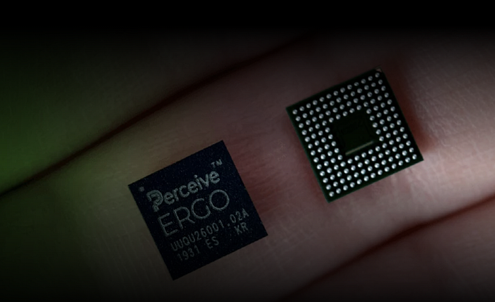
It can apply to video object detection, audio event detection for security (like broken glass), face recognition (like used for the smart door lock), and speech recognition for voice command and remote control, etc … It can run YOLOv3 for up to 246 frames at 30 frames per second while consuming about 20 milliwatts of power.
Blaize
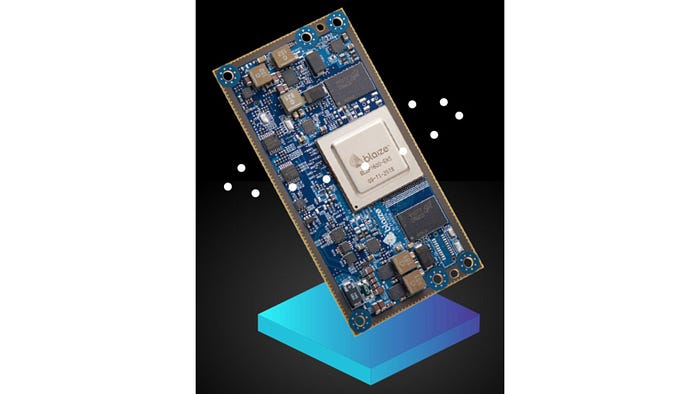
The Blaize El Cano GSP (Graph Streaming Processor) has 16 cores delivering 16 TOPS of AI inference with 7W power consumption. The DNN model can be executed natively on GSP as a graph (graph native). Image data is split into blocks and then processed with a depth-first hardware scheduler. Intermediate data is held in the cache as briefly as possible to minimize RAM access. The GSP is multi-threading and streaming. It can run multiple models concurrently. Here is a video (slightly market-oriented) demonstrating the high-level technology concept.
Stealth Mode Startups
These include NUVIA which has a $53 million Series A funding in late 2019. It mainly focuses on compute performance, power efficiency, and scalability. SiMa.ai’s Machine Learning SoC (MLSoC) is another such company with a claim of breaking the 1000 FPS/W barrier in ML inference.
Why do I choose these companies?
There are plenty of startups and big companies that are important in this field. But there are no clear indicators including performance benchmark or market shares for a fair comparison in the selection process. MLPerf becomes one of the leading benchmarks for Deep Learning. It is a good start but yet, it does not give you a full picture. Indeed, almost everyone claims they perform the best in benchmarking! For metrics like TOPS, I will probably use it to compare products within the same company only. Comparing performance without the proper context is vague. The selection process is quite random here. I do miss out on important big companies and many startups. It is my bad. I have not included vertical embedding systems like those in autonomous driving also. Feel free to add your thoughts to the comment section. Just don’t use that as a marketing channel. Include technical substance on the solution (not marketing pitches). Otherwise, it will be likely removed.